 Much has been written about the increasing shortages of multi-layer ceramic capacitors (MLCC), surface mount (SMT) resistors and other semiconductor devices. Right now we are seeing price increases and greatly extended lead times. In some cases, the delivery time is so long that the component is all but unavailable, and there has been a vast increase in devices notified as ‘end of life’ and due for obsolescence.
Where components can be found, it is quite possible that they will be offered in smaller package sizes than before. According to a recent TTi MLCC Market update manufacturers are migrating to smaller package sizes. We might find, for example, the popular 100nF capacitor soon only being available in 0201 or 01005 packages.
It seems the situation is likely to get rapidly worse rather than better. Given that product still needs to be manufactured and sold, it going to be down to design and manufacturing engineers to come up with solutions, and fast.
So, what are our options?
1. Can we fit smaller SMT components on PCB pads designed for larger devices?
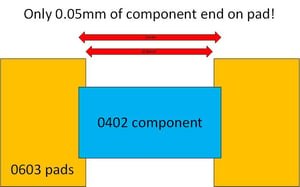
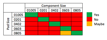
 Maybe. Unfortunately there is no straight answer as it very much depends on the overall PCB design. The component size and the PCB pad design will determine how much of the device can sit on the pad and how good the solder joint can be. Standard sizes for components and pads or ‘land patterns’ are defined by IPC 7531, but for a variety of reasons designs can be slightly different, and maybe more or less favourable to using ‘wrong size’ components. As a worst case you might find something like the following for the smaller components:

If it does appear possible, it will probably be necessary to re-design the solder stencil. Careful stencil design, very accurate component placement and reflow profiling can reduce the risk of unwanted defects such as ‘tombstoning’. Without a change to the stencil aperture, the applied solder will try to ‘wet’ over the whole pad, which being too large for the device can pull it away from the pad.
It might be possible to get the PCB manufacturer to alter the solder resist to cover more of the pad, but again this can present printing problems.
Smaller components might also make it necessary to reduce the stencil thickness from say 5 to 4 thou. A ‘stepped’ stencil could be required to ensure the right amount of solder paste is applied to the right areas of the PCB, or perhaps use solder paste jetting instead of printing.
If you are looking to comply with IPC-A-610 standards then you might find this approach is unsuitable. There could also be implications for longer term product reliability due to the solder joints being less than ideal.
Inspection and test also needs considering. In particular, Automated Optical Inspection (AOI) will need to adjusted. First time pass yields are likely to decrease, and a larger amount of rework may be necessary.
Of course when specifying alternative components their performance characteristics need to be correct too; smaller components may well have different operating voltages, heat dissipation etc. making them unsuitable for your circuit. ‘Track and gap’ requirements might need to be considered.
It is also worth checking that your SMT assembly equipment is capable of placing smaller components as 0402, or even larger, could be the limit for older equipment.
2. Can we re-design the PCB for smaller components?
Yes, and this is probably the preferred option, though much of the above still applies in terms of checking production capability, component characteristics and the need to amend stencils and inspection. Of course testing and approvals processes will also need to be considered.
It might be possible to replace a few components with smaller parts, and keep the rest the same, by using a stepped stencil as discussed above. However if the new smaller components are widely distributed across the PCB, decoupling capacitors for example, then a more extensive re-design might be required to ensure all components are small enough to use the same stencil thickness. Alternatively it may be necessary to consider jet printing the solder paste.
If space allows, designing pads to accommodate two component sizes could help. This could be by having parallel components (with one not fitted) or by adjusting the pad size and gap; though of course consideration needs to be given to the solder joint that can achieved.
So what should we do now?
In summary, the best approach is to discuss and evaluate what is possible with your manufacturing engineers before committing to any smaller components, as they will most probably raise some challenges – and costs – if indeed the parts are useable at all.
Ensuring the electrical integrity of the circuit is maintained is also vital, and of course any testing and/or approvals processes must be planned in.
Most important of all though is to start planning now. Your Electronics Manufacturing Services (EMS) provider may have done a great job so far shielding you from this issue and securing stocks on behalf but there’s a limit to what they will be able to achieve as the months roll by without your input.
