Perhaps the two most popular types of Automated Test Equipment (ATE) used in electronic PCB assembly are In-Circuit Test (ICT) and Flying Probe. But how do you choose the most effective solution for your assemblies and guarantee a test strategy that works best for you?
Much depends on the complexity of your product, of course, and whether you want to add any ‘special features’ on either solution; the following guide highlights the benefits and shortcomings of both types of testing, to help get you started when discussing test strategy with an Electronics Manufacturing Services (EMS) provider.
Product Design
For either solution, in order to achieve a good quality test programme (i.e. good ‘coverage’ – see below) both Computer Aided Design (CAD) data and schematics are required. The CAD data is used to generate the basic test programme, ensuring information is taken from the original design rather than manual interpretation of other data.
Populated and unpopulated sample PCBs (preferably good ones!) are then necessary for fine-tuning the test programmes - ‘debugging’ - and making any fixtures, to ensure the assemblies will physically fit as they should. So where are the differences between each solution when looking specifically at product design?
- Flying Probe machines, like those offered by Takaya, can probe the ends of component pads and uncovered vias to get access to the electrical networks.
- In-Circuit Test (ICT), on the other hand, will require at least a 50thou wide test pad per net, designed into the PCB up front, which is used as a target for the fixed test probe. Ideally, these should be on one side of the PCB as double-sided fixtures are expensive.

Costs
The programming cost itself really depends on the complexity of the assembly, but is broadly similar for either solution, potentially around £2000 or so. When it comes to other charges associated with test, these are the main differences you should be aware of:
Advantages of Flying Probe:- The fixture costs are usually zero, whereas an ICT fixture is mostly in excess of £4000, maybe much more.
- Development lead time is typically less than a week, whereas ICT takes up to 6 weeks for fixture manufacture and programming.
- If your product design changes, only a programme change is required. For ICT however, it might mean a new fixture as well, if components or test pads have moved.
- The actual machine test time is usually less than a minute, so great for getting through larger batches. Flying probe can take several minutes, so is generally more suited to smaller batches.
- ICT is fast so relatively inexpensive, often less than £1 per unit. Flying probe is much slower, so can cost £50 or more per assembly.
Coverage
‘Coverage’ in this case means how much of the circuit you can test in one way or another. Both ICT and Flying Probe carry out what is called ‘manufacturing defects analysis’ (MDA), which covers the majority of the most common process defects that can occur. These include: open circuits (e.g. something not soldered), short circuits, passive component measurements (resistors and capacitors), diode and transistor orientation, and usually, basic supply voltage measurements. So with this feature common to both types of testing platform, what then are the things that set them apart in this area?
Advantages of Flying Probe:- Most Flying Probe systems offer limited optical inspection, whereas ICT fixtures generally don’t. This inspection can add coverage for those components that can’t be accessed electrically.
- Integrated circuits (ICs) can have some powered, even basic functional testing, as well as ‘vectorless’ test to check the soldering of pins to the PCB through a non-contact capacitive probe or plate. Flying probe is pretty much limited to vectorless test.
- ICT can also provide limited analogue and digital measurements; flying probe can’t do much due to the limited number of probes.
Download our Technical Paper 'Design guidelines for in-circuit testability'
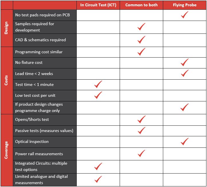
Naturally, the complexity of the product, your monthly demand, and of course budget, will all play an important part in your decision-making process with regard to testing. But, by highlighting the principle benefits and points of difference between these platforms for you, I hope that this post has helped that process along. To further assist we’ve created an easy visual summary of the key features and benefits too:

If you have found this content useful and would like to read more about electronics manufacturing click here to subscribe to our blog.
Image by: Ai.Comput’In
